

-

- alberthink
-
38 发帖1 回复462 积分
- 私信他 + 关注


 楼主
楼主
下面我们就分不同模块来看看micro:bit板上的电气连接和元器件使用。
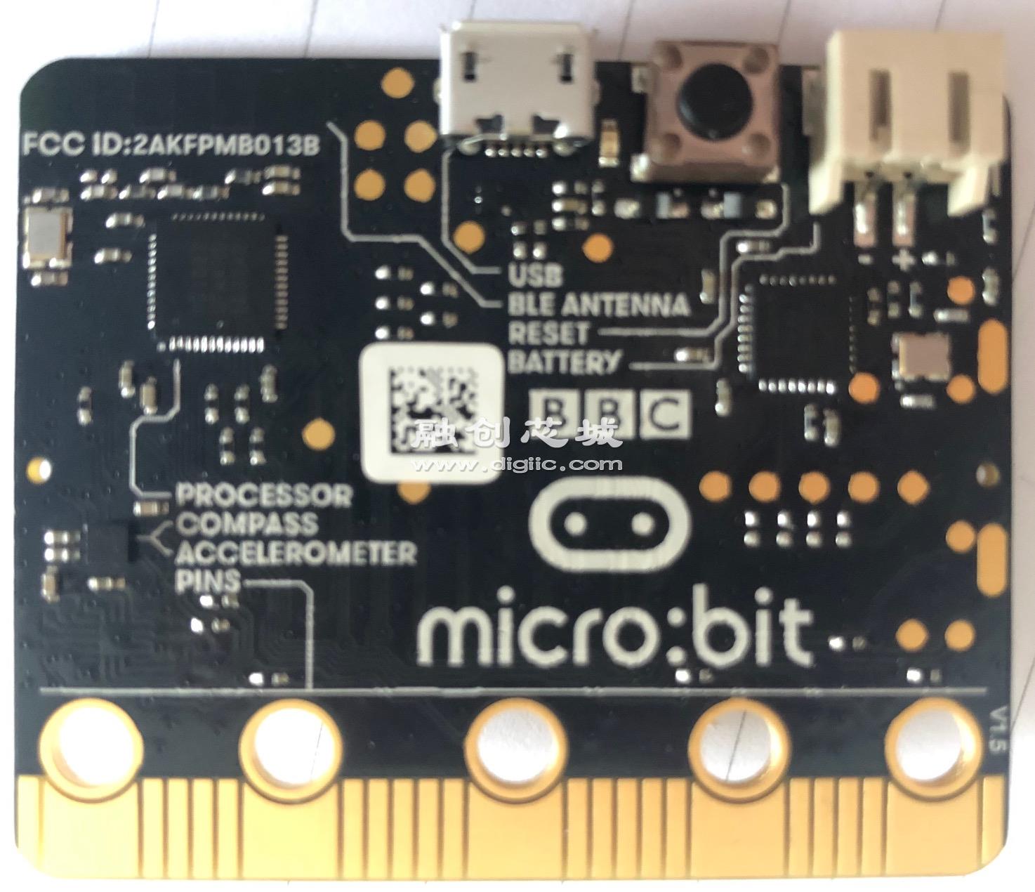
nRF51应用处理器
Nordic的nRF51应用处理器是Microbit用户程序运行的地方。一个单一、完整的应用包含用户代码、runtime代码和蓝牙协议栈是通过片上的闪存直接调用和运行的。所有用户可以访问GPIO均由这个处理器提供。而板上还有蓝牙2.4G信号的天线线路。
| item | details |
|---|---|
| Model | Nordic nRF51822-QFAA-R rev 3 |
| Core variant | ARM Cortex-M0 32 bit processor |
| Flash ROM | 256KB |
| RAM | 16KB |
| Speed | 16MHz |
| Debug | SWD, jlink/OB |
| More Info | here |
蓝牙无线通信
板载2.4Ghz收发器支持Nordic S110 SoftDevice(提供了完全认证过的蓝牙低功耗协议栈)通过蓝牙通信。这使得microbit能和包括智能手机和平板电脑在内的众多蓝牙器件通信。
| item | details |
|---|---|
| Stack | Bluetooth 4.1 with Bluetooth low energy |
| Band | 2.4GHz ISM (Industrial, Scientific and Medical) 2.4GHz..2.41GHz |
| Channels | 50 2MHz channels, only 40 used (0 to 39), 3 advertising channels (37,38,39) |
| Sensitivity | -93dBm in Bluetooth low energy mode |
| Tx Power | -20dBM to 4dBm in 4 dB steps |
| Role | GAP Peripheral |
| Congestion avoidance | Adaptive Frequency Hopping |
| Profiles | 1 BBC micro:bit profile |
| More Info | here |
低阶无线电通信
板载的2.4Ghz收发器支持一系列的无线通信标准,包括专有的Nordic Gazell协议。这个协议提供了在支持该协议的两个microbit之间通过简单的小封包广播接口。这个广播接口出现在众多通过microbit支持Gazell协议的开发语言中。另外,microbit runtime还增加了一个给每一个数据做“组编码”从而允许用户方便简单的控制器件寻址和过滤。
| item | details |
|---|---|
| Protocol | Nordic Gazell |
| Freq band | 2.4GHz |
| Channel rate | 1Mbps or 2Mbps |
| Encryption | None |
| Channels | 101 (0..100) |
| Group codes | 255 |
| Tx power | Eight user configurable settings from 0(-30dbm) to 7 (+4dbm) |
| Payload size | 32 (standard) 255 (if reconfigured) |
| More Info | here |
按键
在microbit正面有两个按钮,背面有一个按钮,均为常开式按压使能触点。背面的按键与KL26接口芯片以及nRF51应用处理器相连实现系统复位。也就是说当背面案件按下时,不论通过电池或是USB供电,处理器都会复位。
前面的按钮A和按钮B可以供用户应用使用。A和B按键都配有软件防抖动误触发功能,同时软件也可以识别短按、长按以及“A+B”同时按下的情况。按键均运行在一个标准的反相器模式:按键松开时上拉电阻送出逻辑“1”而按键按下时送出逻辑“0”。A/B按键都连接到GPIO同时也在microbit的边沿引脚引出。
| item | details |
|---|---|
| Type | 2 tactile user buttons, 1 tactile system button |
| Debounce | (A & B) software debounced, 54ms period |
| Pullup | (A & B) external 4K7, (System) 10K |
显示
LED阵列是5x5排布在板上的,但硬件线路是采用9列3行的矩阵扫描实现的(其中第2行第8列和第2行第9列节点并没有对应到实体的LED)。运行软件重复高速刷新LED阵列使得人眼无法感知闪烁。软件同时也使用了LED行和列引脚来实现光感功能,通过重复切换某些LED的驱动引脚为输入引脚同时采样电压的降落时间来大致估测环境光照的水平。
| item | details |
|---|---|
| Type | minature surface mount red LED |
| Physical structure | 5x5 matrix |
| Electrical structure | 3x9 |
| Intensity control | 10 steps |
| Intensity range | TBC |
| Sensing | ambient light estimation via software algorithm |
| Sensing Range | TBC, 10 levels from off to full on |
| Colour sensitivity | red centric, red is 700nm |
运动传感器
1.5版本microbit采用了一个集成加速度和磁力计的combo芯片提供3轴加速度感测和3轴磁场强度感知。传感器同时包含一些硬件的姿态监测(比方自由落体)以及附加的软件算法实现的姿态感知(比如logo-朝上,logo-朝下,摇晃)。在标准runtime采用的软件算法运用加速度(独立于磁力计)读数来确定板子的朝向。磁力计在使用前必须校准,校准的过程在runtime软件中是自动触发的。器件是通过I2C连接到应用处理器的。
1.5版本的传感器引脚是兼容两个不同运动传感器的:一个是ST的LSM303AGR,另一个是NXP的FXOS8700CQ。microbit DAL通过runtime检测对两种传感器都是支持的。迄今为止,全部的V1.5版本的板载传感器均是采用的LSM303AGR。如果我们要切换到NXP的器件,在一系列的测试完成后我们才会通过microbit DAL邮件组通知大当家。
| item | details |
|---|---|
| Model | LSM303GR |
| Features | 3 magnetic field and 3 acceleration axis , 2/4/8/16g ranges |
| Resolution | 8/10/12 bits |
| On board gestures | ‘freefall’ |
| Other gestures | Other gestures are implemented by software algorithms in the runtime. |
温度传感器
NRF51应用处理器具有一个片上温度传感器。温度在标准runtime软件中可以读取作为环境温度的估计。
| item | details |
|---|---|
| Type | on-core nRF51 |
| Sensing range | -25C .. 75C |
| Resolution | 0.25C steps |
| Accuracy | +/-4C (uncalibrated) |
| More Info | here |
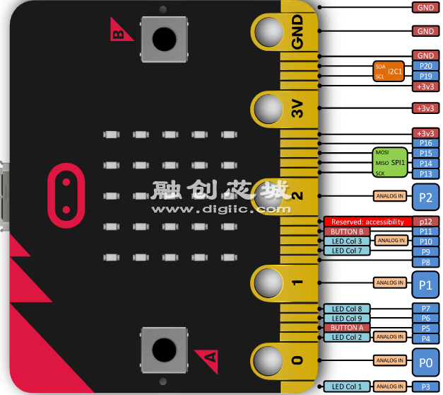
通用I/O引脚
Microbit边沿的连接器从应用处理引出了许多GPIO。其中一些是功能复用引脚,但多数引出引脚可以通过软件设置关闭某些特性而被用作通用IO。nRF51规格书关于GPIO引脚应当在标准驱动电流模式(0.5mA)和高驱动电流模式(5mA)中,但同一时间最多不能有超出三个引脚居于高驱动电流模式。
| item | details |
|---|---|
| Rings | 3 large IO rings and two large power rings, 4mm plug and crocodile clip compatible |
| GPIO features | 19 assignable GPIO pins |
| 2 are assigned to the on board I2C interface | |
| 6 are used for display or light sensing feature | |
| 2 are used for on board button detection | |
| 1 is reserved for an accessibility interface | |
| 19 may be assigned as digital input or digital output | |
| 19 may be assigned for up to 3 simultaneous PWM channels | |
| 19 may be assigned for 1 serial transmit and 1 serial receive channel | |
| 6 may be assigned as analog input pins | |
| 3 may be assigned to an optional SPI communications interface | |
| 3 may be assigned for up to 3 simultaneous touch sensing inputs | |
| ADC resolution | 10 bit (0..1023) |
| Edge Connector | Edge connector |
| Pitch | 1.27mm, 80 way double sided. |
| Pads | 5 pads, with 4mm holes |
| More Info | here |
电源
Microbit的电源系统可以允许通过USB供电,通过接口芯片(其具有片上LDO)供电,或者通过插在顶部的连接器的外接电池供电。同时也可以通过底部边沿引出的3V电源端子供电。该端子也可以用来给其他系统供应小量的电力。
| item | details |
|---|---|
| Operating range | 1.8V .. 3.6V |
| USB current | 120mA max |
| Onboard Peripherals budget | 30mA |
| Battery connector | JST X2B-PH-SM4-TB |
| Battery current | TBC |
| Max current provided via edge connector | 90mA |
| More Info | here |
接口
USB接口芯片管理USB连接同时用来为microbit烧写新代码,发送和接收到你的电脑的串行数据。
| item | details |
|---|---|
| Model | Freescale MKL26Z128VFM4 |
| Core variant: | ARM Cortex-M0+ |
| Flash ROM | 128KB |
| RAM | 16KB |
| Speed | 16MHz |
| Debug capabilities | SWD |
| More Info | here |
USB通信
microbit具有板载USB通信协议,协议是放在接口芯片的固件中的。这个协议支持通过拖放来给Microbit的应用处理器更新代码。它同时也允许串行数据流通过USB接口在microbit应用处理器和主机之间流通,同时它也支持CMSIS-DAP协议用来在线debug。
| item | details |
|---|---|
| Connector | USB micro, MOLEX_47346-0001 |
| USB version | 1.1 Full Speed device |
| Speed | 12Mbit/sec |
| USB classes supported | Mass Storage Class (MSC) |
| Communications Device Class (CDC) | |
| More Info | here |
调试Debugging
接口芯片可以通过采用串行主机工具来debug在应用处理器上运行的代码。它通过4根信号线连接到应用处理器。KL26接口芯片的代码也能通过它集成的SWD软件debug接口来调试,比方说在出厂时写入初始bootloader代码或者在bootloader损坏后的恢复。
| item | details |
|---|---|
| Protocol | CMSIS-DAP |
| Options | JLink/OB (via different firmware) |
| More Info | here |
 回复
回复
 举报
举报
-
- 0000000000000000
-
1888 发帖7917 回复34980 积分
- 私信他 +关注


 回复于 2019-06-30
5#
回复于 2019-06-30
5#


块
导
航
举报
请选择举报类别
- 广告垃圾
- 违规内容
- 恶意灌水
- 重复发帖
