

-

- 0000000000000000
-
1888 发帖7917 回复34980 积分
- 私信他 + 关注


MCP2518FD PRO评估板:CANFD最高8M用户手册/原理图/参考代码等资料汇总分享
用户手册/原理图/参考程序等资料下载见附件,电脑登入
技术交流群:171897584

- 符合ISO11898-1:2015标准
- 支持CAN 2.0B和CAN FD
- 仲裁比特率高达1 Mbps
- 数据比特率高达8 Mbps
- 高达20 MHz的SPI时钟速度
- 31个FIFO可配置为发送或接收
- 32个灵活的滤波器和掩码对象
- 一个传输队列
- 32位时间戳
- 总线运行状况诊断和错误计数器
- VDD:2.7V-5.5V
- 有功电流最大值:12 mA @ 5.5V,40 MHz CAN时钟
- 温度范围:-40°C至+ 150°C
- 封装:VDFN14(可湿性侧翼),SOIC14
- 低功耗模式电流: 10 uA,最大值
-
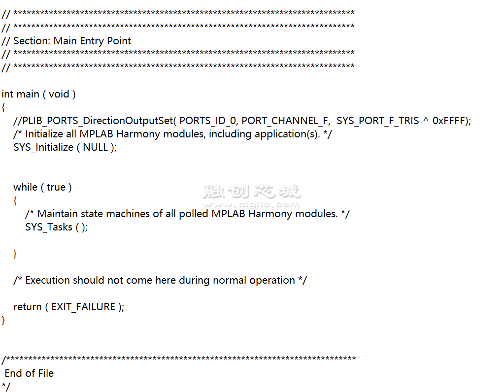
MCP2518FD Prois a complete CAN solution, which can be used as a control node in a CAN network. The Proboard™ is used to provide the microcontroller (MCU) with unrestricted access to the CAN network bus. MCP2518FD Prois equipped with both the control logic and the physical interface ICs. MCP2518FD Proprovides a reliable high-speed CAN interface to the MCU, providing multiple operating modes (CAN 2.0, CAN FD, Listen Only mode, Sleep and Low Power mode…), CAN bit stream processing (decoding and encoding of the CAN messages, error handling…), TX prioritizing, RX filtering, FIFO buffer, interrupt engine, and more.
MCP2518FD prois supported by a mikroSDK compliant library, which includes functions that simplify software development. This Proboard™ comes as a fully tested product, ready to be used on a system equipped with the mikroBUS™ socket.
 回复
回复
 举报
举报
-
- 0000000000000000
-
1888 发帖7917 回复34980 积分
- 私信他 +关注
 楼主
|
回复于 2020-01-10
沙发
楼主
|
回复于 2020-01-10
沙发
TABLE OF CONTENTS
10. Third party support
11. mikroSDK
12. Resources
13. Downloads
The physical layer is implemented by using a separate IC, which provides increased robustness, required for the automotive applications. It features three operating modes, remote wake-up via the CAN, and offers ideally passive behavior on the CAN bus when it is powered off. These features allow MCP2518FD Proto be used for the development of a wide range of automotive diagnostic applications, even on MCUs that do not natively support CAN interface.
-
- 0000000000000000
-
1888 发帖7917 回复34980 积分
- 私信他 +关注
楼主
|
回复于 2020-01-10
2#
HOW DOES IT WORK?
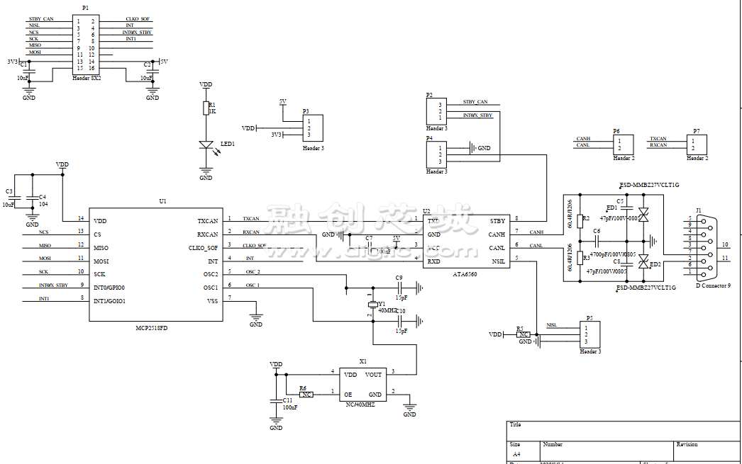
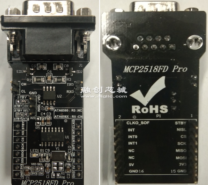
The Proboard™ consists of a transceiver IC, a low-level physical layer IC (PHY) which provides a physical connection with the CAN bus itself, and a CAN controller IC, which is used as an interface between the MCU and the PHY IC. MCP2518FD Prouses the ATA6560/X, a high-speed CAN transceiver with Standby mode, and the MCP2518FD, CAN FD controller with the SPI interface, both ICs by Microchip.
The role of the CAN bus controller is to provide arbitration, message framing, message validation, error detection, message filtering, and so on. Among all other tasks - it is used to provide clearly formatted CAN data for the application layer, running on the host MCU.
-
- 0000000000000000
-
1888 发帖7917 回复34980 积分
- 私信他 +关注
楼主
|
回复于 2020-01-10
3#
CAN TRANSCEIVER
As the physical layer (PHY) IC, the ATA6560/1,ATA6562/3, a high-speed CAN transceiver with Standby mode, by Microchip. This IC provides the physical connection with the CAN bus and as such, it provides high resistance to electrostatic discharge and other electromagnetic phenomena, with its bus pins protected against transients, often encountered in the automotive environment. It allows communication speed up to 5Mbps. For the CAN bus device, it is important not to block the entire bus by permanently setting itself as the dominant node. For this reason, the PHY IC has the TX time-out function. It is also important to have defined bus pin states of nodes at all times. The ATA6560/1 PHY IC has its functional behavior predictive under all supply conditions. The ATA6560/1 is powered directly from the mikroBUS™ 5V power rail. This IC can work in several modes:
Normal mode is engaged when the STBY pin is at the logic LOW level, while the TXD pin is held to a HIGH logic level. While in the Normal mode, bus biasing is set to half the supply voltage, and the data can be transmitted and received via the CANH and CANL bus lines.
If the STBY pin of the ATA6560/1 is set to a HIGH logic level, the PHY IC will enter the Standby mode. While in Standby mode, the device is not able to transmit or correctly receive any data. The internal TX and HSC (high-speed comparator) sections are turned off, reducing the power consumption. Also, the bus lines are biased to the GND level. While in Standby mode, the device actively listens to the CAN bus traffic, looking for a valid wake-up pattern.
Since the STBY pin directly controls the operating mode of the PHY IC, it is routed to the onboard SMD jumper labeled as the STBY, allowing more than one way of control. This SMD jumper allows choice between connecting the STBY pin to the GND directly (LOW logic level), or allowing it to be controlled via the source selected by yet another SMD jumper, labeled as STBY SEL: control via the AN pin of the mikroBUS™, or the INT0/GPIO pin of the CAN control module IC.
For more CAN transceiver information please referthe web:https://www.microchip.com/design-centers/can
-
- 0000000000000000
-
1888 发帖7917 回复34980 积分
- 私信他 +关注
楼主
|
回复于 2020-01-10
4#
CAN BUS CONTROLLER
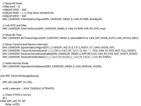
The MCP2518FD, CAN FD controller with the SPI interface, also by Microchip, is used to control and shape the CAN bus data traffic. While the PHY IC provides CAN communication on a basic - physical level, the MCP2518FD takes care of all the communication and data formatting. It manages the proper decoding and encoding of messages, data arbitration, message transmission prioritizing and filtering, provides the FIFO buffer for the messages, and so on. This IC can even provide a clock source to the host MCU, reducing the number of needed components to a minimum. On one end, it uses the SPI to communicate with the host MCU, while on the other end, it uses RXCAN and TXCAN pins to communicate with the PHY layer IC. The MCP2518FD supports CAN frames in classic format (CAN2.0B), as well as the CAN Flexible Data Rate format (CAN FD), as specified in ISO11898-1:2015.
CAN FD controller IC contains 2K of integrated RAM, which is used as the message buffer. Besides this, it also contains a number of SFR registers, used to configure and operate the controller IC, including the configuration of the INT/GPIO pins, their direction and polarity, configuration of the clock section, operating mode (including the Low Power mode for the MCP2518FD IC), FIFO control and message filtering, and so on. All the registers are 32bit wide. The datasheet of the MCP2518FD IC can be consulted for a comprehensive list of all the SFR registers and their functions. However, the provided library contains functions which can be used with MikroElektronika compilers. The included example application demonstrates the use of these functions, and it can be used as a reference for custom development.
There are three interrupt pins routed to the mikroBUS™: INT, INT0, and INT1, pins of the MCP2518FD IC are routed to the INT, TX and RX pins, respectively. While the INT pin is always an interrupt output pin, used to alert the MCU of the interrupt event that is enabled and has its flag bit activated, INT0 and INT1 pins are used to alert the MCU about the RX and TX events (if these interrupts are enabled), or as the GPIO pins. INT0 pin is also routed to the onboard SMD jumper labeled as STBY SEL, so that can be used to control the PHY IC standby mode. All interrupt pins are active low.
-
- 0000000000000000
-
1888 发帖7917 回复34980 积分
- 私信他 +关注
楼主
|
回复于 2020-01-10
5#
CLKO pin from the MCP2518FD IC is routed to the PWM pin of the mikroBUS™. This pin can be used to provide the clock output for the host MCU. Before it is used, it has to be configured via the SFR registers. It is derived from the input clock, generated by the onboard chip oscillator. The onboard SMD jumper allows frequency selection between 20MHz and 40MHz.
This IC can be interfaced directly to the MCU pins. To provide support for both the 3.3V and 5V operating MCUs, the Click board™ is provided with the onboard SMD jumper. This jumper determines only the logic voltage level and it is routed to both the VCC pin of the MCP2518FD IC and the VIO pin of the ATA6560/1. However, for proper operation of the Click board™, both 3.3V and 5V rails from the mikroBUS™ are used.
The Click board™ comes equipped with the standard DB-9 connector, making the interfacing with the CAN bus simple and effortless.
-
- 0000000000000000
-
1888 发帖7917 回复34980 积分
- 私信他 +关注
楼主
|
回复于 2020-01-10
6#
SPECIFICATIONS
|
Type |
CAN |
|
Applications |
It can be used for developing reliable custom CAN applications by using a wide range of MCUs, even if the used MCU does not include an integrated CAN module. |
|
On-board modules |
MCP2518FD, CAN FD controller with the SPI interface from Microchip; ATA6560/1, high speed CAN transceiver with Standby mode, from Microchip |
|
Key Features |
Expands the existing MCU with the reliable and robust CAN connectivity option. Support for both CAN 2.0B and CAN FD frames, high speed CAN communication up to 5 Mbps, integrated DB9 connector... |
|
Interface |
GPIO,SPI |
|
Compatibility |
mikroBUS |
|
Click board size |
M (31.8 x 60.7 mm) |
|
Input Voltage |
3.3V or 5V |
-
- 0000000000000000
-
1888 发帖7917 回复34980 积分
- 私信他 +关注
楼主
|
回复于 2020-01-10
7#
PINOUT DIAGRAM
This table shows how the pinout on MCP2518FD Pro corresponds to the pinout on the mikroBUS™ socket (the latter shown in the two middle columns).
|
Notes |
Pin |
Pin |
Notes |
||||
|
Standby control IP |
STBY |
1 |
AN |
PWM |
16 |
CLKO |
Clock OP |
|
|
NS(only for ATA6560) |
2 |
RST |
INT |
15 |
INT |
Interrupt OP |
|
Chip select |
CS |
3 |
CS |
TX |
14 |
INT0 |
Int/GPIO 0 / ATA6560/1StdBy |
|
SPI Clock |
SCK |
4 |
SCK |
RX |
13 |
INT1 |
Int/GPIO 1 |
|
SPI data OP |
MISO |
5 |
MISO |
SCL |
12 |
NC |
|
|
SPI data IP |
MOSI |
6 |
MOSI |
SDA |
11 |
NC |
|
|
Power supply |
+3.3V |
7 |
3.3V |
5V |
10 |
+5V |
Power supply |
|
Ground |
GND |
8 |
GND |
GND |
9 |
GND |
Ground |
-
- 0000000000000000
-
1888 发帖7917 回复34980 积分
- 私信他 +关注
楼主
|
回复于 2020-01-10
8#
ADDITIONAL PINS
|
Name |
I/O |
Description |
|
TX_CAN |
I |
CAN transmit |
|
RX_CAN |
O |
CAN receive |
|
CANL |
I/O |
CAN low line |
|
CANH |
I/O |
CAN high line |
JUMPERS AND SETTINGS
-
- 0000000000000000
-
1888 发帖7917 回复34980 积分
- 私信他 +关注
楼主
|
回复于 2020-01-10
9#
|
Designator |
Name |
Default Position |
Description |
|
JP1 |
VIO.SEL. |
Left |
Logic level voltage selection: left position 3V3, right position 5V |
|
JP2 |
STBY |
Right |
Selection of the Standby function: left position - ON, right position - STBY SEL configuration |
|
JP3 |
STBY SEL |
Left |
STBY input source selection: left position - STBY pin, right position - mikroBUS™ INT0 pin |
|
JP4 |
20/40MHz |
Right |
Clock frequency selection: left position - 20MHz, right position - 40MHz |
-
- 0000000000000000
-
1888 发帖7917 回复34980 积分
- 私信他 +关注
楼主
|
回复于 2020-01-10
10#
LEDS AND BUTTONS
|
Designator |
Name |
Type |
Description |
|
J1 |
- |
CONNECTOR |
DB9 connector for CAN |

块
导
航
举报
请选择举报类别
- 广告垃圾
- 违规内容
- 恶意灌水
- 重复发帖
